Design Services

The quality of any one package design has become significantly more critical in influencing the performance
of final electronics products. In regard to package design, the importance of chip carrier designs is highly
significant, specifically leadframe or substrate designs. Aside from working towards higher performance, cost
continues to be a critical factor to the success of a product.
Leadframe Design
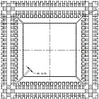
ASECL offers design services for mature packages e.g. PDIP, SOIC, PLCC, QFP, L/TQPF, Exposed Pad L/F, Fused
L/F, L/F with Drop-in Heat Spreader, Leadframe for MCM, QFN, tailor-made L/F for special applications
(including prototype engineering), etc.

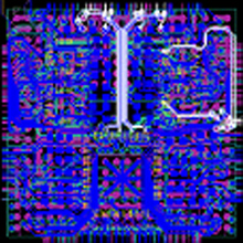
Substrate Design
ASECL, as one of the first BGA mass production factories in the world, provides a wide spectrum of BGA
designs with differing substrate technologies. T/L(F)BGA in ASECL’s proprietary strip outline provides best
material utilization and highest productivity which is potentially a most cost-effective design. MCM substrate
design with side-by-side/stacked die and passive components has been a mainstream requirement in ASECL. With
all these design options, cost and technology are balanced either with regular two/four layer substrate or
advanced GPP, build-up substrates for flip chip or high density wire bonding device applications.
Hip Carriers for Opto Electronics and MEMS
With the developments in opto-electronics and microelectronic machineries, ASECL is developing chip carrier
design suited for these kind of end-customers. Close relationships and fast responses to customers greatly
ease customer’s backend costs, and ultimately shorten development cycle times.
Design Tools
The most powerful and commercially used design tools are utilized to enhance ASECL’s design capability.
Output design formats are widely compatible with customers’ existing software. Remote communication and
discussion through file exchanges are easy and effective. As a result, ASECL truly becomes an absolute virtual
design center.
Hip Carriers for Opto Electronics and MEMS
Design/layout tools:
• Cadence APD 14.2
• AutoCad 2000
• CAM 350 PC Berber-II (RS-274-x)
Design input information:
• Microsoft office format netlist (pad coordinates, net name, ball no.)
• Die information (CAD file or Microsoft office format).
Design output file format:
• *.dwg, *.dxf, *.mcm, *.anf, *.pdf, Gerber file, GDSII etc.
©
ASE ChungLi, All Rights Reserved. Terms of
Use