Bumping & WLCSP
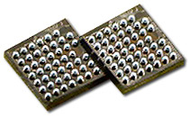
Product Overview
ASECL's WLCSP technology is licensed from FCT, has been qualified since 2000, and to date,
over several million wafers have been shipped to customers around the world. ASE ChungLi provides a variety of
wafer bumping services including Standard (FOC), Repassivation (REP) and Redistribution (RDL) using different
type of dielectric material for standard eutectic bump and lead free bumps. Our bumping capabilities and
technologies mean that we can offer customers a full turn-key solution, by providing services ranging from
product design to drop shipment, including bumping, wafer grind, marking, wafer sort, singulation, and tape
and reel, or waffle pack. Our turnkey solution provides customers with the opportunity to meet demanding
time-to-market demands. ASECL's goal is to provide the most cost effective and reliable WLCSP package solution
possible to all our customers.
Applications
WLCSP provides the best solution required for compact, light, thin and highly dense packaged
ICs, such as applications for communication products like cellular phones, PDAs and other portable
electronics.
Features
Package Offering
| Printed Bump & WLCSP | |
| Wafer size | 150mm, 200 mm and 300mm( Q4,2006) |
| Pad metallization | Al / Si / Cu, Al / Cu , CUP |
| UBM Type | AL/NiV/Cu, Ti/NiV/Cu |
| Wafer Technology | 0.13 FSG |
| Process | FOC, Re-passivation, Redistribution, Ultra CSP® |
| Solder composition | Eutetic 63/37, Pb-free SAC405, SAC105 |
| Printed Bump pitch ( mininum ) | Array: 150 um |
| Peripheral: 130 um | |
| Drop Ball Bump pitch ( mininum ) | Array: 400 um |
| Die size | 1x1mm²~20x20mm² |
| Bump count | 4~3600 bumps / die |
| Bump height | 70um~300um |
| Bump height | 70um~300um |
| Plated Bump |
| Technology available by Q3'2010 |
| 12" WLCSP available by Q2'2010 |
Reliability
| Item | Condition | Duration | Sampling | Criteria | Standard | Status |
| Precondition | 30°C 60%RH |
45/lot | No Open/ Short Failure No Die Crack No Delamination |
JEDEC A113-A Level 3 |
Pass | |
| HAST | 130°C 33.5psig 85% RH |
100hr | 45/lot | No Open/ Short Failure |
JEDEC 22, A110 |
Pass |
| Temperature Cycling Test |
-55°Cto+125°C 30 min/cycle Air to air |
100cycle 200cycle 500cycle 1000cycle |
45/1ot | No Open/ Short Failure No Die Crack No Delamination |
JEDEC 22, A104-A Condition B |
Pass |
| Temperature Humidity |
85°C 85%RH |
168hr 500hr 1000hr |
45/lot | No Open/ Short Failure |
JEDEC 22B A101-A |
Pass |
| High Temperature Storage |
150°C | 168hr 500hr 1000hr |
45/lot | No Open/ Short Failure |
JEDEC 22B A103-A |
Pass |