Leadless LGA
Product Overview
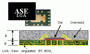
Land Grid Array (LGA) uses laminate substrate to form the landing pad and the exposed pad for performance enhancement. It is essentially BGA but without the solder balls, and has the advantages of flexible routing and the capability of multi-chip module over other leadless packages. LGA is also a thinner (down to 0.66 mm) and lighter CSP. LGA technology was developed for lead free solution and spacing reduction on a mother board. This type of package has a chip size solution based on mature laminated substrate technology and material.
LGA is suitable for high performance ICs like single chip, logic and memory. Common applications for this type of package includes telecommunication products, personal digital assistants (PDAs) and memory cards.
LGA is suitable for high performance ICs like single chip, logic and memory. Common applications for this type of package includes telecommunication products, personal digital assistants (PDAs) and memory cards.
Features
Package Offering
| LGA | LLGA | TLGA | VLGA | WLGA | WLGA | Ultra LGA | |
| Mold | 1.6 | 1 | 0.8 | 0.7 | 0.54 | 0.45 | 0.37 |
| Substrate | 0.52 | 0.36 | 0.26 | 0.26 | 0.26 | 0.22 | 0.22 |
| 0.38 | 0.26 | ||||||
| Total thickness | 2.2 max | 1.4 max | 1.2 max | 1.0 max | 0.8 max | 0.8 max | 0.6 max |
| Pitch | General pitches= 0.4, 0.5, 0.65, 0.8 | ||||||
| Customized pitches also available | |||||||
| Package Size | Standard body sizes = 3x3 ~ 27x27 | ||||||
| Other rectangular body sizes also available | |||||||